
Seagate’s new M.2 carrier card has generated quite a buzz since the company gave an introductory demonstration of the product at the 2016 OCP conference in early March. Not only is the card widely touted as the fastest SSD in the world, the product also was developed in collaboration with hyperscale customers under the Open Compute Project (OCP). This collaboration means that in addition to it being the fastest PCIe SSD in the world, but it is also designed with a cloud SSD cost and is much more energy-efficient than products designed for traditional enterprise.
This blog posting details a presentation I gave at the conference in which I discussed how the OCP and Facebook have influenced not just the development of our new product, but also how the collaboration promises to allow the wider adoption of SSD technology in general. Watch a video of the presentation below:
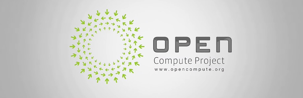
A big part of OCP is about driving out cost and going forward with an open source infrastructure to power the internet. OCP also makes it easier for everyone to adapt to new technologies faster than they could otherwise. Since its inception in 2012, OCP has had a dramatic influence on the development of CPUs, networking and storage. In terms of the storage space, OCP efforts have centered on SSD because it is such a new area and there is so much demand for them in hyperscale.
The stages in the process for the development of a cloud SSD can be summarized as follows:
- Take what already exists and enable more direct interfacing.
- Define the properties of a cloud SSD.
- Enable broad community adoption.
The first stage was to take components that already existed and make them interface with one another more directly. One of the first things that happened where OCP had a big impact was the release of a specification that allowed more direct communication between PCIe flash devices and the BMC inside the server. This allowed, among other things, temperature monitoring of the flash and the ability to adjust fans on an OCP server. Giving servers the ability to monitor chip temperatures directly may seem trivial or mundane on the surface, but that capability has led to a power reduction of approximately 35W, which, given the rapid decline in SSD costs, has translated into a significant savings of 15% of the total cost of deploying flash in the data center.
The second stage was to define the properties of the cloud SSD. This step involved the following three activities.
- Establishment of a base standard
Microsoft did a great job of defining what it wanted out of cloud SSDs. It took a community-based approach to determine what these SSDs needed to be able to do for hyperscale. It first gave vendors, like Seagate, an indication of a base standard it was looking for (i.e., M.2 form factor, terabyte capacity, and a base interface it wanted to support). - Definition of permitted deviations
Basically, Microsoft was looking at a client standard that would stretch into hyperscale, so it identified a few things that didn’t make sense for hyperscale deployments and it revised the requirements. For example, it determined that the standard requirement to support unpowered data retention of three months for SSDs didn’t fit the realities of the hyperscale world—in hyperscale data centers, nobody leaves the infrastructure off for anywhere near that amount of time. The cloud SSD didn’t need to be designed for a traditional enterprise architecture, so one of the easiest things that could be done was to establish that one week of data retention would be fine. - Address additional requirements
The final step in defining the properties of a cloud SSD was to address additional requirements that are needed but that aren’t already defined in specification. In this case, we were looking at predictable and consistent latency, which is needed for hyperscale environments.
The previous stages were big steps to help power cloud SSDs to the next level. The huge challenge, however, was to foster broader community adoption–challenging because in order to do so, a server built around the M.2 form factor was necessary. Although M.2 might be interesting, it was not designed to go into currently shipping enterprise servers easily: It has a gumstick shape, its thermals were not great, the amount of power available on the board real estate is limiting and most servers don’t have any NVMe M.2 slots!
The third stage, then, was to take the cloud SSD setup and somehow make it more broadly available. This is where Seagate’s new carrier card comes in.
Seagate is able to encourage wider adoption of M.2 cloud SSDs by making it unnecessary to build specialized servers to accommodate them. One of its carrier cards has four M.2s installed directly on it–this means there is no need for PCIe switches, which add cost and power. Seagate worked with the community to define different BIOS settings so that the single card can be interpreted as four discreet x4 PCIe devices, allowing savings of 8W of power and $50 of BOM. The traditional standard doesn’t allow this, as a x16 slot is supposed to show up as single PCIe device. But Seagate made it possible to take the great cloud SSD base product and make it easy to use in standard OCP servers.
The innovations that went into developing and fostering a wider adoption of an exceptional cloud SSD did not come about overnight, nor did they happen in a silo. Although relatively quick by traditional scales of measurement, the advances came about in the stages that I enumerated above. More importantly, they were made possible by a close collaboration that Seagate had with Facebook and the OCP community. As such, the development and evolution of this product should serve as a great example of the kinds of hardware innovation can be possible by working with the OCP community